Description
Welcome to Well-Tech - one of the leading manufacturers and suppliers of PCB products in China. Our factory is engaged in PCB manufacturing and offering customized back drilling high-end printed circuit board made from fr4 tg170 material with 2.0mm thickness at competitive price. High reliability, strong diversity and expert advice are our characteristics. Please contact us if you have inquiry.
Products description:
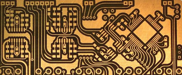
Back drilling PCB: The back drilling process removes stubs from plated-through-holes (vias). Stubs are the unnecessary / unused portions of vias, which extend further than the last connected inner layer. Back drill can be applied to any type of circuit board where stubs cause signal integrity degradation, with minimal design and layout considerations.
Products specification:
Layers: 8
Material /Laminate: FR4 TG170
Board thickness: 2.0mm
Copper weight: inner & outer 1oz
Finishing: ENIG
|
The procedure for back drilling as beow, |
|
material cutting->inner layer process->etching->AOI->Brown Oxide->pressing->drilling->PTH->outer layer process->inspection->pattern plating->back drilling |
|
The parameter for back drilling as below, |
|
1. Minimum back drilling through hole: 0.2mm |
|
2. Maximum big hole (NPTH portion) for minimum back drilling: 0.5mm |
|
3. The depth accuracy tolerance: +/-0.1mm |
|
4. The minimum back drilling depth: 0.2mm |
|
5. Backing drilling hole should be per side Min. 4mil bigger than through hole. |
|
6. Blind hole, through hole to be back drilled double side is workable. |
|
Sketch map as below, |