Description
Welcome to Well-Tech - one of the leading manufacturers and suppliers of PCB products in China. Our factory is engaged in PCB manufacturing and offering customized high quality iso9001 and ul approved multilayer via in pad pcb at competitive price. High reliability, strong diversity and expert advice are our characteristics. Please contact us if you have inquiry.
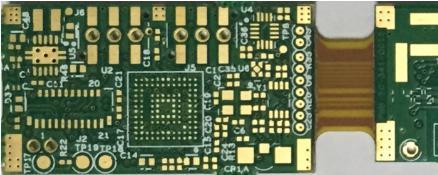
Products description:
VIA IN PAD PCB: Vias in pad is normally to be plugged with non-conductive epoxy and then plated caps. Filling non-conductive epoxy/resin is more cheaper than filling copper. And this filling gives better result for soldering as it can avoid tin flowing into holes when assembly.
Products specification:
Layers: 8
Material /Laminate: FR4 TG170
Board thickness: 1.2mm
Copper weight: 1.5/1/1/1/1/1.5oz
Finishing: ENIG
Via in Pad technical advantages can be divided into 2 categories. Firstly, reduce the spacing of hole to hole as well as board size. Secondly, solve the problems with the wiring conductor and improve the wiring density.
|
The briefly process for VIA IN PAD as beow, |
|
material cutting→drilling→PTH→plating→non-conductive epoxy plugging→polish→drilling through hole→PTH→plating→outer layer pattern→plating→etching→solder mask→surface finish→routing→testing→FQC→package. |